Metal stamping project aims at cutting manufacturing costs

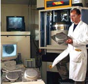
NIST post doctoral research fellow Mark Iadicola examines a sample of sheet metal that has been tested with NIST’s new formability testing station. <br>Photo by Barry Gardner/NIST
With new, one-of-a-kind test equipment, National Institute of Standards and Technology (NIST) researchers aim to stamp out costly, delay-causing errors in the design of dies used to make sheet-metal parts ranging from car hoods to airplane wings to pots, pans and cans.
The U.S. auto industry alone is estimated to spend more than $700 million a year on designing, testing, and correcting new dies for its latest models, each containing about 300 stamped parts shaped by dies and presses. About half of the total goes for remedying unanticipated errors–manifested as wrinkles, splits, excessive thinning or other defects.
By fitting NIST’s metal-stamping test station with an X-ray stress measurement system, the Institute’s materials scientists now can make detailed maps of stresses and strains as sheets of steel and other metals are punched, stretched or otherwise shaped to achieve the desired part geometry. According to project leader Tim Foecke, the system can measure stress and strain behavior in many different directions while the sheet is being stretched in two directions simultaneously, a condition most commonly seen in forming operations. Current methods extrapolate from strain measurements taken from tests that stretch the sheet in only one direction. As a consequence, newly designed dies often must undergo successive rounds of refinement to correct for these simplifications in computer models.
U.S. automakers and producers of steel, aluminum and other metals, including developmental ones, are supplying Foecke’s team with samples for testing and evaluation. The project will result in a novel database of materials’ properties that designers can feed into computer models for predicting whether would-be dies can form particular metals into specified shapes, within tolerances. Project findings might point the way to new metal-forming methods.
Media Contact
More Information:
http://www.nist.gov/All latest news from the category: Process Engineering
This special field revolves around processes for modifying material properties (milling, cooling), composition (filtration, distillation) and type (oxidation, hydration).
Valuable information is available on a broad range of technologies including material separation, laser processes, measuring techniques and robot engineering in addition to testing methods and coating and materials analysis processes.
Newest articles

Parallel Paths: Understanding Malaria Resistance in Chimpanzees and Humans
The closest relatives of humans adapt genetically to habitats and infections Survival of the Fittest: Genetic Adaptations Uncovered in Chimpanzees Görlitz, 10.01.2025. Chimpanzees have genetic adaptations that help them survive…

You are What You Eat—Stanford Study Links Fiber to Anti-Cancer Gene Modulation
The Fiber Gap: A Growing Concern in American Diets Fiber is well known to be an important part of a healthy diet, yet less than 10% of Americans eat the minimum recommended…

Trust Your Gut—RNA-Protein Discovery for Better Immunity
HIRI researchers uncover control mechanisms of polysaccharide utilization in Bacteroides thetaiotaomicron. Researchers at the Helmholtz Institute for RNA-based Infection Research (HIRI) and the Julius-Maximilians-Universität (JMU) in Würzburg have identified a…


