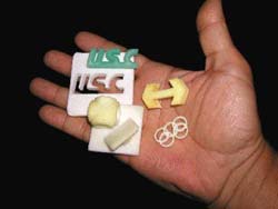
New USC process offers faster, cheaper 3D ’printouts’

Desktop manufacturing for home desks seen
A University of Southern California inventor has created a machine that can produce 3-dimensional “printouts” in plastic and even metal more quickly and cheaply than widely-used existing systems.
The new machine is a significant improvement on the laser sintering machines now widely used around the world to build complex 3D forms from computer files, according to its creator, Professor Behrokh Khoshnevis of the USC School of Engineering’s Daniel J. Epstein department of Industrial and Systems Engineering.
One patent has been granted and others are pending on the process, which may eventually put 3D object-making within reach of home offices.
Both traditional laser sintering and Dr. Khoshnevis’ “Selective Inhibition of Sintering” (SIS) process start with CAD (“computer aided design) three-dimensional form creation software.
The three-dimensional shapes visualized in the computer are re-visualized as stacks of very thin virtual layers. Then, each virtual layer is transformed into a real one.
Sintering machines build up objects by spreading a less- than-1 millimeter thick layer of powdered plastic or other material in a work area, and then melting (“sintering”) selected areas, guided by the computer pattern. The process is repeated multiple times, with unmelted powder shaken off or blown away at the end of the process.
The result is to gradually build up complex forms, layer by layer. Such structures as free rolling balls inside of cages, for example, can easily be made.
The objects created were once almost exclusively used as molds or prototypes for die-casting, stamping or other traditional mass-production processes, and this role gave the name “rapid prototyping” to such processes. But with the increasing sophistication of techniques, some companies now use R-P processes – and particularly laser sintering — for what is now called “direct manufacturing” or “desktop manufacturing” of final products.
Existing machines use a moving laser beam traveling over the work area to do the melting. SIS, for “Selective Inhibition Sintering” instead automatically treats some of the powder applied to resist bonding with adjacent particles under heat, and then exposes the entire piece to uniform, high-intensity heat. Untreated areas of powder sinter. Treated areas do not.
Various anti-sintering materials can be used, including salt water.
Khoshnevis says the SIS process has several advantages over laser machines. The lasers and scanners used in such machines are extremely expensive (up to $100,000 each), short-lived, and energy intensive, he notes, while the heat source for an SIS can be a low- tech gas flame, or an inexpensive electrical heater filament. The cheap, high heat possible with the SIS process makes the use of metals as well as plastics feasible.
Finally, because lasers have to scan out the entire work area, turning on and off to melt the needed areas, they are intrinsically slower in building up pieces, with large, complicated pieces requiring many hours, or even days. The SIS machine can complete a layer in as little as 15 seconds.
The advantages of the process make it possible to see a wider range of use for such machines. “Down the line,” says Dr. Khoshnevis, “home offices may have them, right alongside the printer.” Shops may have similar, heavier duty units, he said, filling work niches now held by lathes and milling machines.
Khoshnevis now has a working prototype machine, the performance of which he has demonstrated at various conferences.
Khoshnevis’ research was supported by a grant from the National Science Foundation.
Behrokh Khoshnevis Web site http://www-rcf.usc.edu/~khoshnev/
Media Contact
All latest news from the category: Process Engineering
This special field revolves around processes for modifying material properties (milling, cooling), composition (filtration, distillation) and type (oxidation, hydration).
Valuable information is available on a broad range of technologies including material separation, laser processes, measuring techniques and robot engineering in addition to testing methods and coating and materials analysis processes.
Newest articles

Parallel Paths: Understanding Malaria Resistance in Chimpanzees and Humans
The closest relatives of humans adapt genetically to habitats and infections Survival of the Fittest: Genetic Adaptations Uncovered in Chimpanzees Görlitz, 10.01.2025. Chimpanzees have genetic adaptations that help them survive…

You are What You Eat—Stanford Study Links Fiber to Anti-Cancer Gene Modulation
The Fiber Gap: A Growing Concern in American Diets Fiber is well known to be an important part of a healthy diet, yet less than 10% of Americans eat the minimum recommended…

Trust Your Gut—RNA-Protein Discovery for Better Immunity
HIRI researchers uncover control mechanisms of polysaccharide utilization in Bacteroides thetaiotaomicron. Researchers at the Helmholtz Institute for RNA-based Infection Research (HIRI) and the Julius-Maximilians-Universität (JMU) in Würzburg have identified a…


