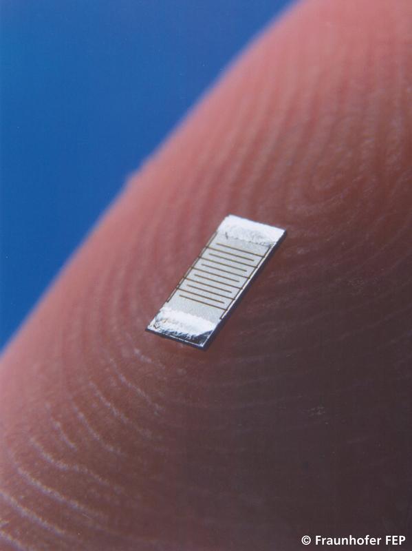
Devarnishing by electron beam

Fabrication of operational microfeatures through precision electron beam devarnishing © Fraunhofer FEP
Precise, selective devarnishing of layers from a substrate plays an important role in numerous industrial production processes. The manufacture of precision resistors, sensor fabrication, and production of electronic displays and monitors can be mentioned here as key examples.
A typical job would be to etch operational electronic layers such as resists on plastic, ceramic, or glass substrates at the micron-scale in order to trim characteristics to the desired level, such as precise balancing of electrical resistances, setting sensor values, as well as defining the smallest units of operation.
It is important during this step that devarnishing of the layer be as residue-free as possible while causing a minimum of thermal and mechanical stress to the carrier substrate, which can be a real challenge particularly in the case of plastics.
Beam tools offer crucial advantages here, as they provide the necessary accuracy without contacting the work piece during processing. The laser is a tool that has become standard in many fields of application. It ablates or blasts away the intended areas of the layer by intense inputs of pulsed energy.
Fraunhofer FEP will be presenting the electron beam as an alternative though far less familiar beam process – despite its diverse opportunities for application – to a broad public as part of “Devarnishing”, this year’s main theme at the parts2clean trade show.
The scientists at Fraunhofer FEP have been involved with the design and manufacture of suitable beam sources for many decades and develop tailored solutions for specific processing jobs jointly with clients.
Specialized properties of electron beam technology open up several important advantages compared to other processes for devarnishing layers. In contrast to the laser, whose energy is quickly absorbed at the surface (especially in the case of metallic layers), absorption of the electron beam takes place in the bulk of the layer.
This enables the penetration depth of the beam to be exactly set according to layer thicknesses that are present. The irradiated bulk is thereby heated directly rather than relying on indirect thermal conduction processes and is removed from the beam track as molten liquid. In this respect, the electron beam does not differentiate between optically transparent and optically absorptive layers, so that one and the same beam source can be used for both types of materials.
Thanks to the selective depth mentioned above and being able to very quickly direct the continuous beam, thermal stresses on the substrate can be kept very small. This enables it to be used on flexible plastic substrates. For micron-level work, the electron beam can be steered and diverted about 10 to 15 times faster than a laser beam at the same working distance.
“The electron beam diameter can be matched to the application, which expands its possibilities for utilization even more. The diameter can even get down to the nanometer range and is being employed especially for high-precision electron-beam devarnishing by means of locally induced gas-phase etching”, explains Benjamin Graffel, one of the scientists in the department Electron Beam Processes at Fraunhofer FEP. “This is already being used for repairing lithography masks in microelectronics, for example.”
The biggest disadvantage frequently mentioned for electron beam technology is the necessity of using vacuum engineering. However, a vacuum actually delivers some important prerequisites for precise devarnishing of thin layers: the absence of air prevents oxidation of adjacent areas during thermal processing, experience indicates trimming resistances is considerably more accurate and reproducible without the presence of humidity, and contamination of the substrate is reduced.
Fraunhofer FEP is a member of the Fraunhofer Cleaning Technology Alliance that dedicates itself to devarnishing, among other topics. The process chain of cleaning technology comprises more than just different cleaning processes. Upstream processes help avoid contamination or reduce the effort and expense of cleaning. Downstream processes include monitoring the effectiveness of cleaning as part of quality assurance, auxiliary cleaning agents, and environmentally sound disposal of contaminants. The expertise of the Fraunhofer institutes covers the entire process chain of cleaning technology. The Fraunhofer Cleaning Technology Alliance bundles and coordinates the relevant expertise of the Fraunhofer institutes. In this way, all of the processes across the entire field of cleaning technology are covered. The Fraunhofer institutes provide a unique range of services for industrial customers.
Fraunhofer FEP at parts2clean 2016
Talk
Wednesday, June 1
Session: Deburring and Devarnishing
Devarnishing – If the functional layer becomes a contaminant!
Dipl.-Phys. Frank-Holm Rögner, Head of Department Electron Beam Processes
Press contact:
Mrs. Annett Arnold
Fraunhofer Institute for Organic Electronics, Electron Beam and Plasma Technology FEP
Phone +49 351 2586 452 | annett.arnold@fep.fraunhofer.de
Winterbergstraße 28 | 01277 Dresden | Germany | www.fep.fraunhofer.de
Media Contact
All latest news from the category: Trade Fair News
Newest articles

First-of-its-kind study uses remote sensing to monitor plastic debris in rivers and lakes
Remote sensing creates a cost-effective solution to monitoring plastic pollution. A first-of-its-kind study from researchers at the University of Minnesota Twin Cities shows how remote sensing can help monitor and…

Laser-based artificial neuron mimics nerve cell functions at lightning speed
With a processing speed a billion times faster than nature, chip-based laser neuron could help advance AI tasks such as pattern recognition and sequence prediction. Researchers have developed a laser-based…

Optimising the processing of plastic waste
Just one look in the yellow bin reveals a colourful jumble of different types of plastic. However, the purer and more uniform plastic waste is, the easier it is to…


