Silver circuits on foil allow curved touchscreens

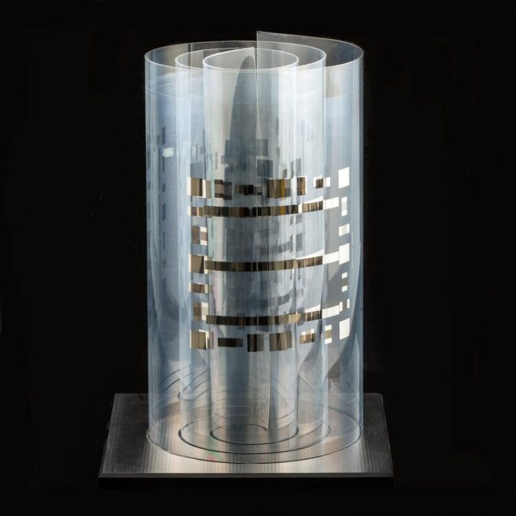
Photochemical Metallization allows conductor paths even on flexible foils as well as on stretchable silicone. Source: Gabi Klein, INM; only free within this context
Mobile phones and smart phones still have not been adapted to the carrying habits of their users. That much is clear to anyone who has tried sitting down with a mobile phone in the back pocket: the displays of such devices are rigid and do not yield to the anatomical forms adopted by the people carrying them.
To allow typing and swiping even on curved smartphones, touchscreens and electric conductor paths have also to be curved. Therefore INM – Leibniz Institute for New Materials has developed a technique, which allows such conductor paths even on flexible foils as well as on stretchable silicone.
INM will be presenting the so called photochemical metallization on this year’s Hannover Messe at the Stand B46 in hall 2 from 24 April to 28 April.
For the proper functioning of touchscreens in smart phones or tablets, microscopically fine conductor paths are required on their surfaces. At the edges of the appliances, these microscopic circuit paths come together to form larger connective pads. Until now, these different conductive paths had to be manufactured in several steps in time-consuming processes.
With the photochemical metallization this is now possible in one single step on flexible substrates. The process offers, has several benefits: It is fast, flexible, variable in size, inexpensive and environmentally friendly. Furthermore additional process steps for post-treatment are not necessary.
For the new process, the foils are coated with a photoactive layer of metal oxide nanoparticles. “After that we apply a colorless, UV-stable silver compound,” Peter William de Oliveira, Head of Optical Materials explains. By irradiation of this sequence of layers, the silver compound disintegrates on the photoactive layer and the silver ions are reduced to form metallic, electrically conductive silver. In this way, paths of varying sizes down to the smallest size of a thousandth of a millimeter can be achieved.
This basic principle allows conductive paths to be created very individually. “There are different possibilities we can use depending on the requirements: ‘Writing conductive paths’ using UV lasers is the process which is particularly suitable for the initial customized prototype manufacture and testing a new design of the conductive path. However, for mass production, this method is too time-consuming,” the physicist de Oliveira explaines.
The researchers are currently working intensely on a further method, the usage of transparent stamps. “These stamps push out the silver compound mechanically; conductive paths then only occur where there is still silver compound,” de Oliveira stated. Since the stamps are made of a soft plastic, they can be arranged on a roll. Because they are transparent, researchers at INM are now working on embedding the UV source directly in the roll. “Thus, the initial steps for a roll-to-roll process would already have been taken,” the Head of Optical Materials group concluded. It would therefore be possible to manufacture conductive path structures of various sizes on foils on a large scale.
Your expert at INM
Dr. Peter William de Oliveira
INM – Leibniz Institute for New Materials
Head Optical Materials
Head InnovationCenter INM
Phone: +49681-9300-148
OptiMat@leibniz-inm.de
INM – Leibniz Institute for New Materials, situated in Saarbrücken, is an internationally leading centre for materials research. INM conducts research and development to create new materials – for today, tomorrow and beyond. Research at INM is performed in three fields: Nanocomposite Technology, Interface Materials, and Bio Interfaces. INM is an institute of the Leibniz Association and has about 240 employees.
Media Contact
All latest news from the category: Trade Fair News
Newest articles

A ‘language’ for ML models to predict nanopore properties
A large number of 2D materials like graphene can have nanopores – small holes formed by missing atoms through which foreign substances can pass. The properties of these nanopores dictate many…

Clinically validated, wearable ultrasound patch
… for continuous blood pressure monitoring. A team of researchers at the University of California San Diego has developed a new and improved wearable ultrasound patch for continuous and noninvasive…

A new puzzle piece for string theory research
Dr. Ksenia Fedosova from the Cluster of Excellence Mathematics Münster, along with an international research team, has proven a conjecture in string theory that physicists had proposed regarding certain equations….


